Solving Jane Street's "Can you reverse engineer an ASIC" puzzle
A note on AI: the reverse engineering, analysis and decisions are mine. I used AI to write/ check code and to help with visualisation scripts, not to solve the puzzle.
Contents
- Setting up and initial attempts
- Reading the hints
- Diving deeper into the cones
- The two format latches
- Further structural exploration
- Looking inside the chip
- The impulse sweep
- A stroke of luck
- What the puzzle actually is
Introduction
Hi there. I’m Aaron. Originally from NZ, I moved to Australia to study a Bachelor of Electrical Engineering at USYD (Graduating mid 2028). I’m interested in FPGAs and anything computing really so this puzzle really caught my eye.
Jane Street’s 2026 puzzle, “Can you reverse engineer an ASIC?”, is literally what the title says. They hand you the final mask of a chip. That is every metal, routing and transistor layer, plus a few sample test inputs and outputs. Our job is to reverse engineer it. The task breaks into three steps. Firstly, recover the netlist from the raw layout. Secondly, work out what the circuit actually does. Lastly, drive it with the right input so it outputs the answer string, which is what you submit.
Warmup
I started by doing the warmup, building the tools and getting familiarised with the various formats (GDS, LEF, DEF). I then pulled the sky130 PDK, built and instantiated the Verilog equivalent. I chose to use cocotb with verification since I’m the most familiar with it. Finally, I verified the warmup not only on the correct addition output, but also wrote a testbench to confirm it does not assert correct in any of the wrong cases.
Puzzle
Setting up and initial attempts
I took the puzzle GDS and ran it through the same pipeline into Verilog, then wrote checkers to confirm the netlist was connected properly. Along the way I found the anomaly of one unconnected cell. Additionally, looking at the provided VCD inputs in GTKWave, the input is a 121 bit stream on I, sampled on each rising clock edge while enable is high. The output comes back on O[7:0], 8 bits per cycle. This can be viewed as one ASCII character at a time since an invalid attempt streams “TRY AGAIN” on O[7:0] and never asserts success. The chip also streams other messages for different inputs, which I cover my findings in the easter eggs section.
After extraction I could see the chip itself (with the help from AI for some visualisations). I first split the die into its registers and its combinational logic to see the overall anatomy of the chip. The ports are traced through the metal layers, so the inputs come in on the left and the outputs leave on the right. Visualisations helped me a lot here and were the ultimate key to my success, so expect many diagrams (pls zoom in if words are too small).
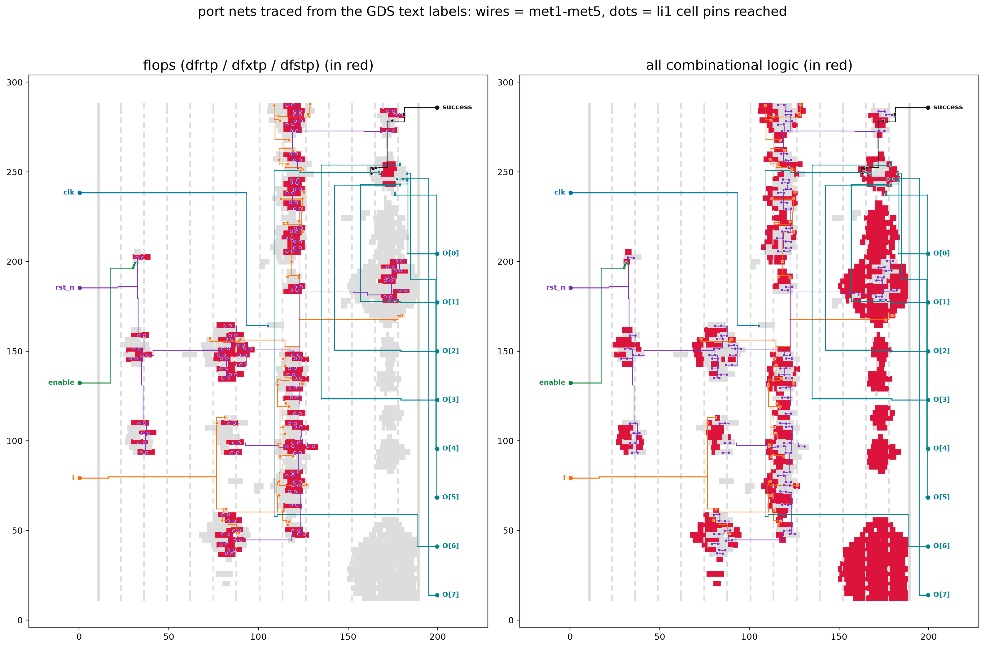
From investigating the sample input (covered in the easter eggs section below), I first thought the puzzle was simply a word checker where each character was an 11 bit word: 7 ASCII bits with 4 bits of zero padding. Therefore, I came up with a few 11 letter words that fit the theme of some of my initially discovered easter eggs and AI helped me extend the list.
Some examples are:
SAGITTARIUS
ORIONS BELT
NIGHT SKIES
STARS ABOVE
JANE STREET
MILKY WAY
Words were also tried with various capitalisations and spacings.
I encoded each as ASCII with the same padding and sent them through a cocotb testbench into the reconstructed chip. However, that did not bear any fruit. Afterwards I tried different words, capitalisations and casings but success was never asserted and the chip said “TRY AGAIN” for all of them.
Reading the hints
Following these blind attempts, I went back to the article posting to gain some sense of direction. The blog said that “The circuit is physically arranged to hint at its functionality,
so look closely at the layout” and that “There is one section of the design that is
used to generate the output but does not affect the [success] output. You can
safely ignore it.” Therefore, I first traced which cells the input actually touches on
the way to success, i.e. the fan-in cone. I also wanted to trace a subset of the fan-in cone, the cells that reach the
success flop within a single clock cycle, which I call the success cone. The
success flop is X228. We first have the entire die after extraction:
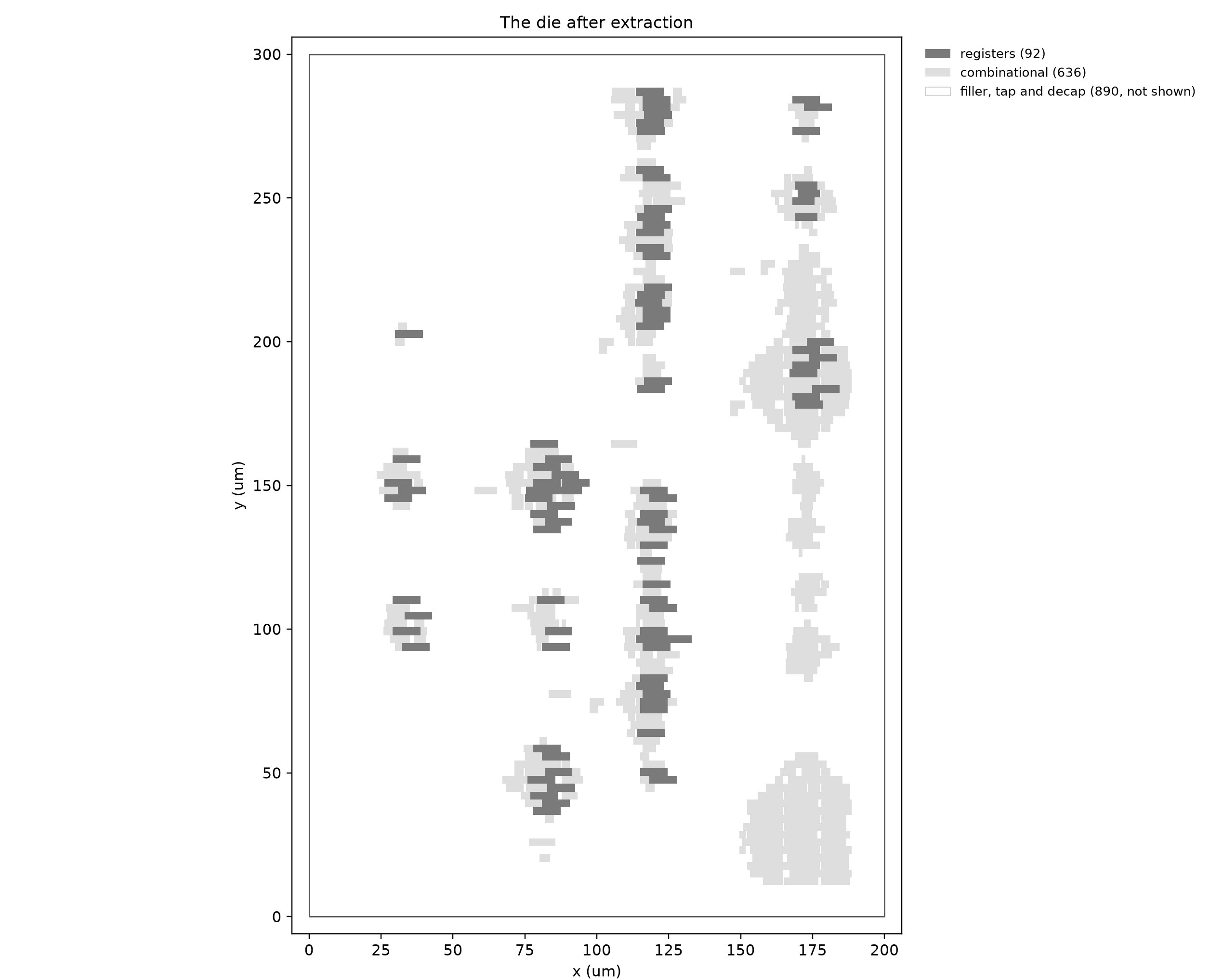
Where the output generator can be ignored. Hence catagorising the fan in cone along with the success cone:
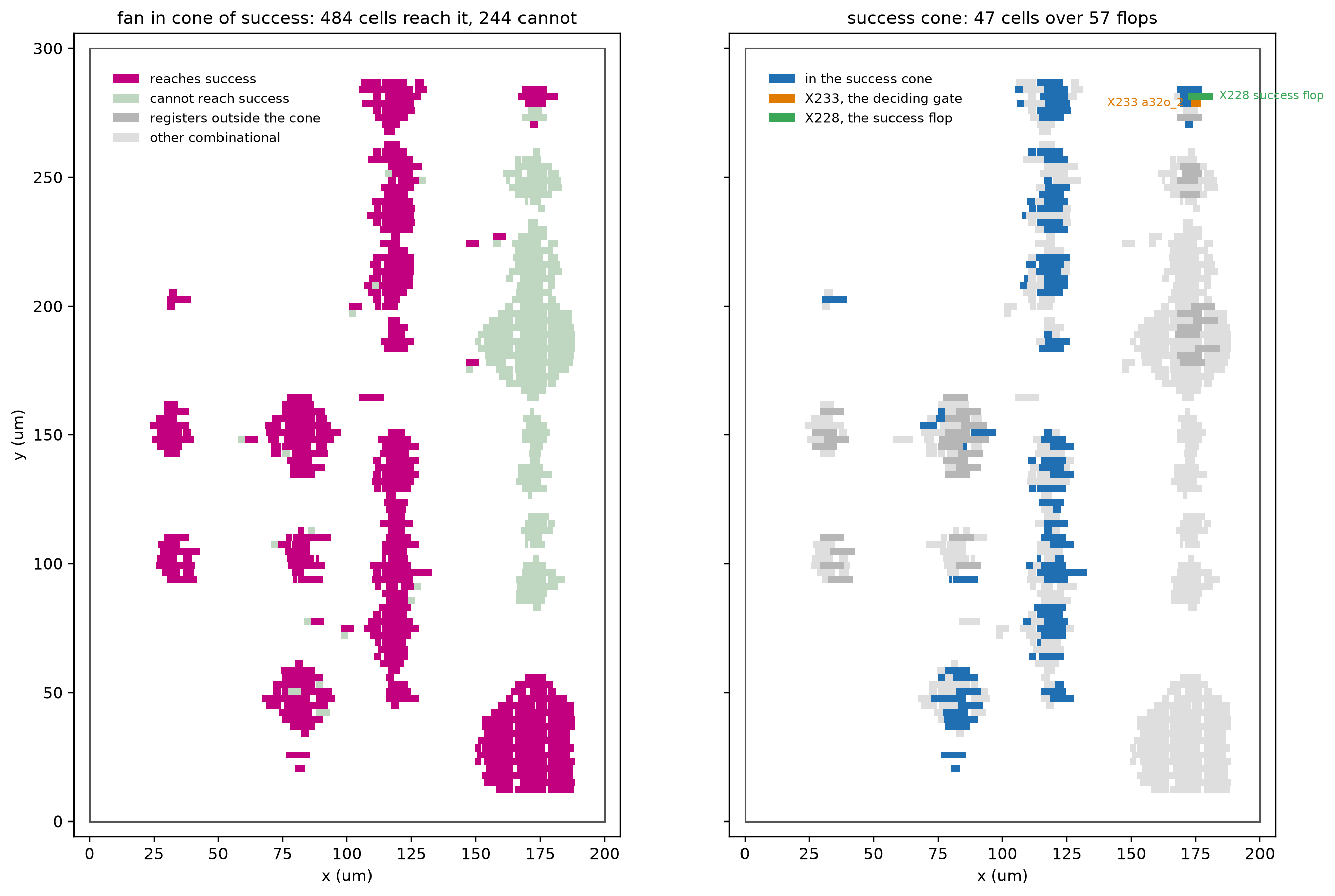
And we can get some characteristics of both cones:
- Fan-in cone. Of the 728 logic cells, 484 can reach
successand 244 cannot. The 244 are the output generator the blog told me to ignore. - Success cone. Walking back from
X228and stopping at flop boundaries gives 47 combinational cells over 57 stored bits. So the pass condition is a one cycle function of 57 flops, an end of stream comparison.
Diving deeper into the cones
Analysing the success cone, it is nearly all AND logic feeding one gate in front
of the success flop. That makes it invertible by hand: an AND forced to 1 pins
every input to 1, a NOR forced to 1 pins every input to 0, and an inverter just
flips the requirement through. No gate in this cone is ever asked for the value
that leaves a choice, so I could push success = 1 backwards through all 47 gates
and every input came out uniquely determined.
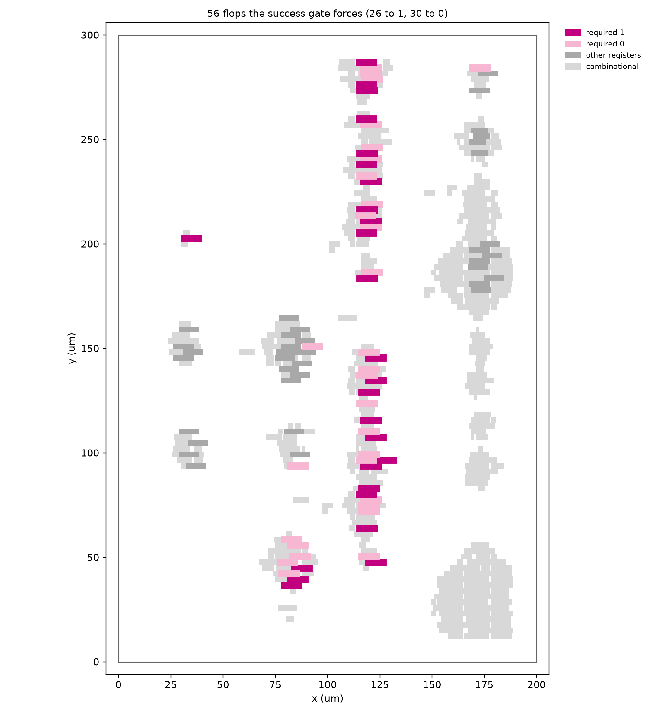
Thereby I wrote a program that created required_state.json: the exact value each of the 56 flops within the success cone must hold for success to subsequently assert high. The required state here is a goal we can approach, but not the answer to the puzzle.
Looking inside the chip
At this point, I needed a tool to help me iterate and visualise multiple ideas quickly. Therfore, with the great help of AI tooling, I quickly built an interactive viewer where I hand it an 11 by 11 grid of 0s and 1s and it streams those 121 bits into the extracted netlist using a cocotb testbench.
# grid.txt: 11 rows, each an 11-bit frame, the left bit is shifted in first
10000000000
01000000000
00100000000
00010000000
00001000000
00000100000
00000010000
00000001000
00000000100
00000000010
00000000001

# in puzzle/interactive:
make          # stream the grid in and print the output ASCII
make image    # also draw which cells lit up, to temp.png
It prints the ASCII the chip streams back on O[7:0] and outputs an image of which cells/ registers were touched, gradient colour coded by when they were first touched by the signal. As an example, streaming in a full grid of ones lights up almost every cell (and gives us a different output):
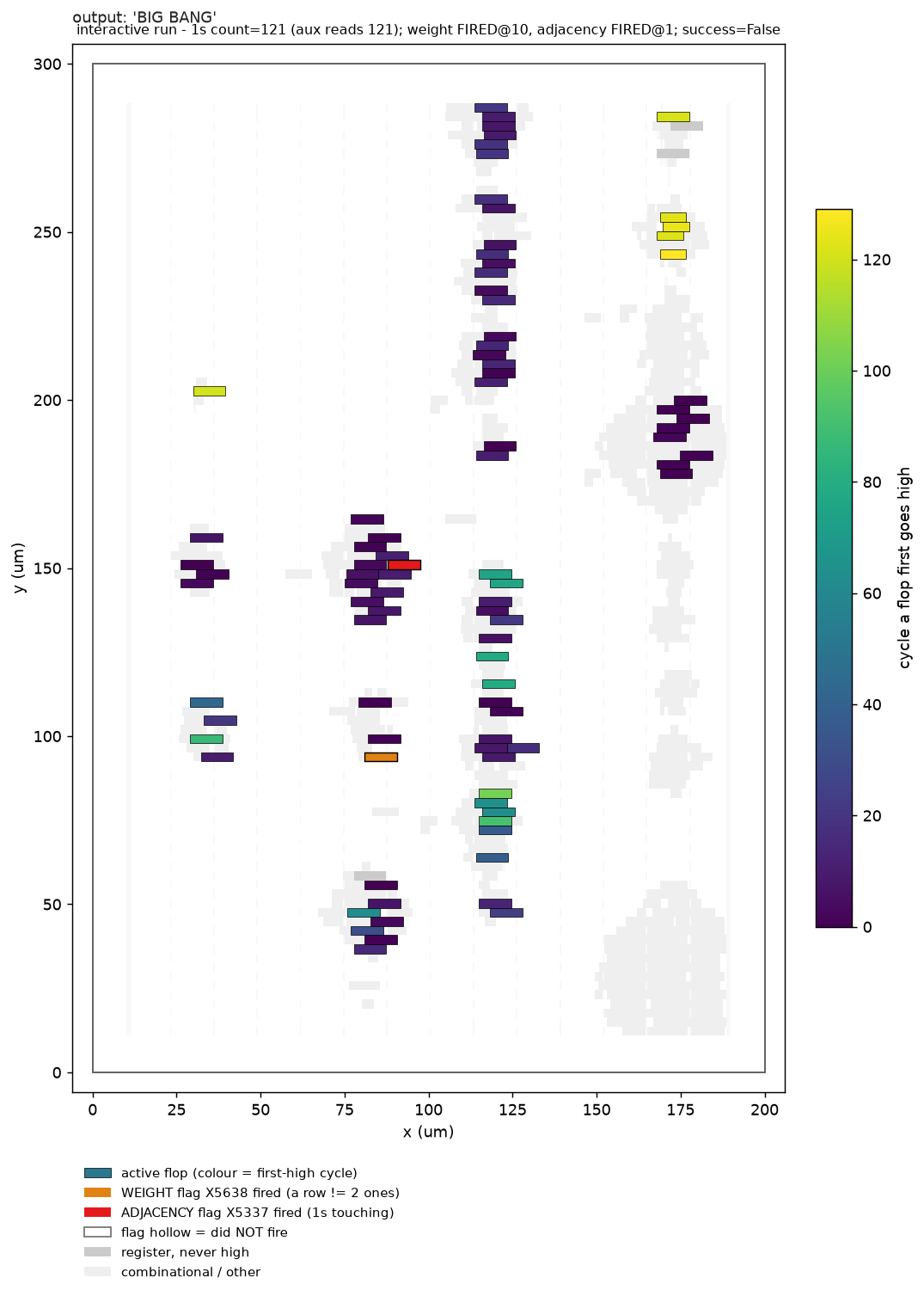
This turned many random ideas into a one command experiment where I could physically see which sections of the enigmatic chip activated and when.
The two format latches
From earlier easter egg investigation, I already knew the input arrives as a stream of 121 bits, which can be interpreted as 11 frames of 11 bits. Feeding frames of different weights and watching the whole chip, register
X5638 stayed low only when a frame held exactly two 1s. Any other count latched
it high and it stuck. Testing all 55 weight 2 symbols in all 11 positions, every
one passed and every other weight failed. So X5638 can be interpreted as a sticky “bad weight”
flag.
During a wider hunt on valid inputs, X5337 showed up. It latched whenever two 1s
sat next to each other in a frame. At the time I read this as a simple no horizontally adjacent
bits rule, only later realising it sat behind a 12 stage shift register which is discussed later on.
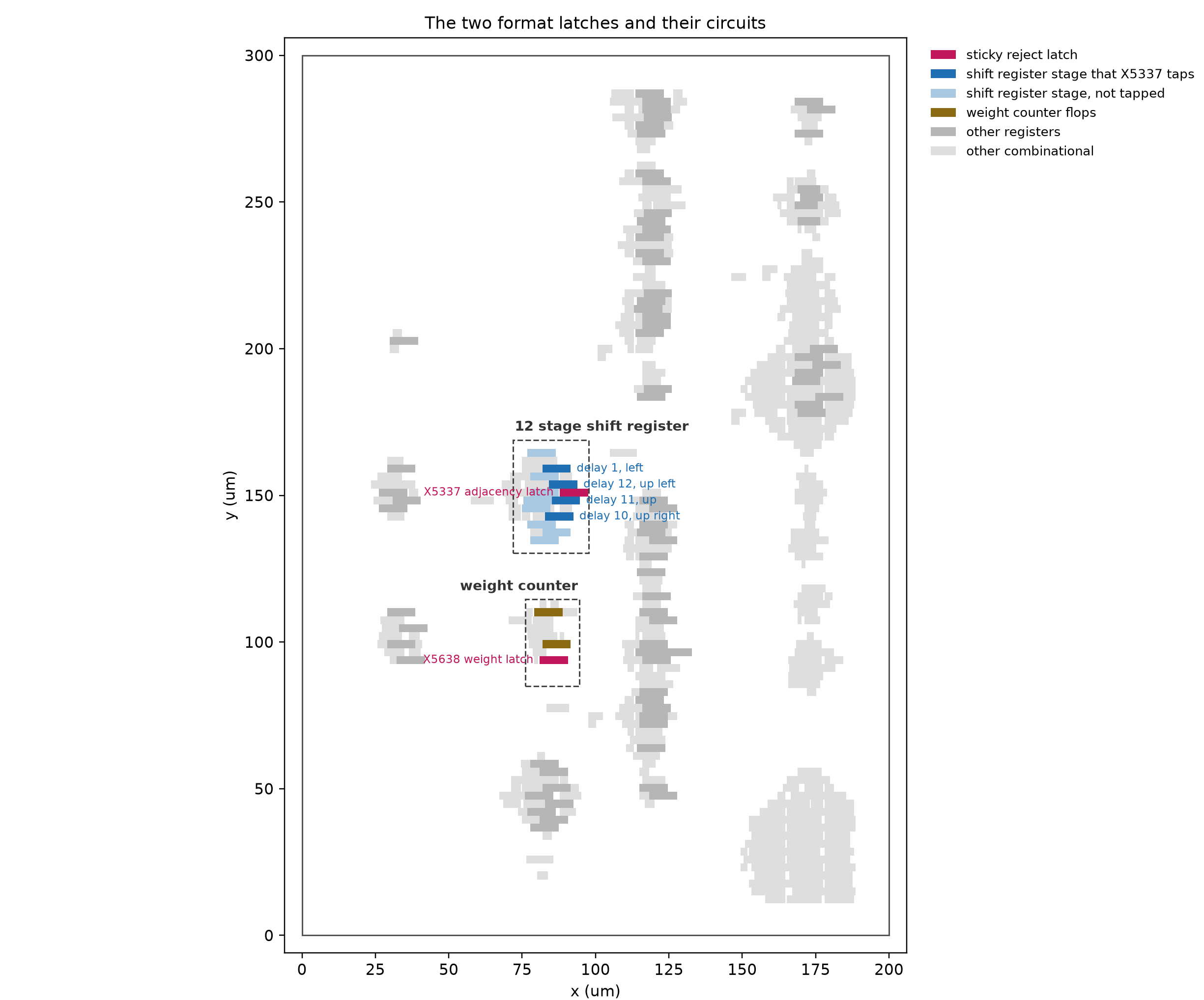
Comparing back to required_state.json, both latches are in the required state and must be off for success, which thereby gives us the first two constraints: exactly weight 2 per frame, and no two bits adjacent. I initially thought of brute forcing the input space however, the space is far too large to brute force. Weight 2 gives 55 symbols per frame, and dropping the 10 side by side symbols leaves 45:
45^11 = about 1.5 x 10^18 streams
At around 0.4 seconds per attempt on my machine that is roughly 19 billion years. Brute force was never on the table. Therefore I kept reading into the structure, since I still did not truly understand the chip, only some rules on its input.
Further structural exploration
Hence I dove deeper into the layout. Firstly, I chose to look into the two large vertical banks that share the same narrow strip of x = ~125 (um), one above the other: Bank A up top and Bank D below. I named them from some previous labelled regions (regions A, B, C, D and so on) of an earlier layout sketch on paper and the names stuck.
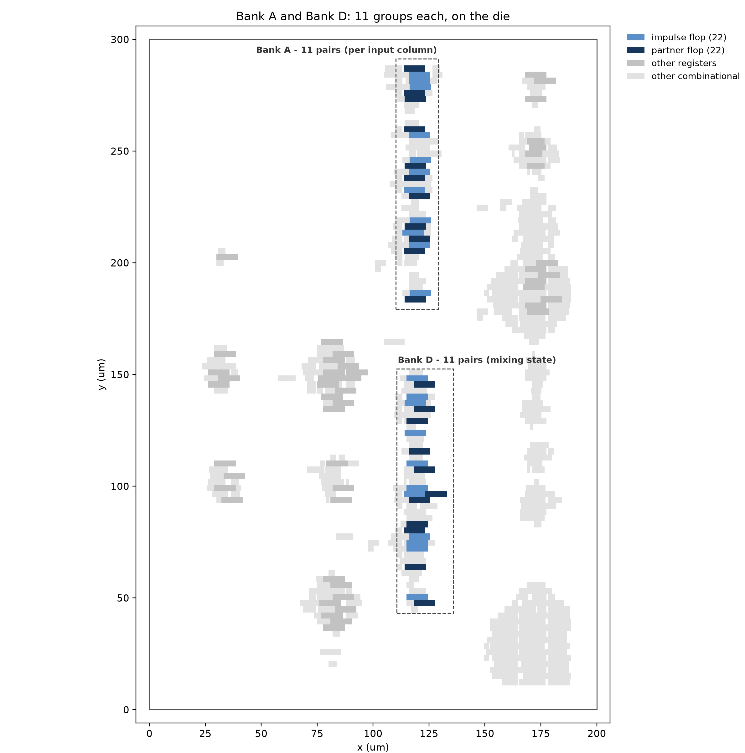
From my setup, I had two things to work with. One was a list of every cell with its position on the die. The other was the extracted netlist, the graph of what drives what.
From there I noticed the flops in these banks were part of the required state, so I took their names and inspected their connectivity. I went to them and walked back through the netlist to see what each one reads. They fell into pairs. Each flop read only itself, its partner and one shared block of 9 flops that every pair also read. That gave 22 clean pairs, which split evenly into two banks of eleven, Bank A and Bank D. The banks did not read the shared block equally. Bank A flops attached to only 5 of the 9, while Bank D flops attached to all 9.
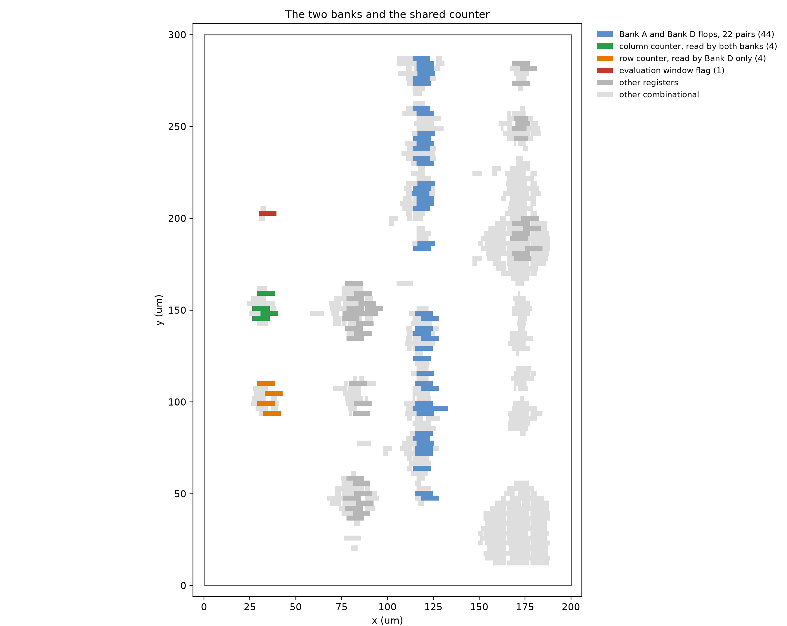
I then looked at what that shared block was. Its nine flops never saw the input and read only each other. Eight of them are part of some sort of counter and the ninth is an evaluation/ enable window flag, connected to the counter and enable and going high near the end. That flag flop is the only one of the nine in the required state, since the final compare lands on the window it marks. The counter itself is two 4bit fields. One is a column count that cycles every frame, the other a row count that ticks once per frame. That explains the 5 / 9 split. Bank A only needs the column, so it reads the column field plus the flag. Bank D needs the full position, so it reads both fields and the flag. Overall:
-
Bank A, 11 pairs. Small update logic, lightly gated by the counter, sitting close to the input. This felt like staging.
-
Bank D, 11 pairs. Much heavier logic, fully driven by the counter. Its update logic is the large combinational block in the bottom right corner, set apart from the flops it drives. This was clearly where the real work happened, though I could not yet understand it.
One result that shaped my thinking: there is not a single adder anywhere in the design. Combined with the input arriving one bit at a time, that ruled out the chip doing any arithmetic on it. That likely rules out anything cryptographic too.
A few other structures I discovered and investigated:
- Large combinational block in the bottom right. Bank D’s update logic, sitting apart from the flops it drives.
- Weight counter. The two flops behind
X5638, doing the per frame count. - Adjacency chain.
X5337behind a 12 stage shift register, comparing the current bit only against delays 1, 10, 11 and 12. Laid out as an 11 by 11 grid those are exactly the four already seen neighbours: left, up, upper left and upper right. The other four are checked when they take their turn. So the real rule is no two 1s touching anywhere on the grid, diagonals included. This is where I stopped seeing a stream and started seeing a grid. - Global count. A ripple counter whose value is just the total number of 1s in the whole input.
The impulse sweep
This was the move that helped me crack the puzzle. Inspired by my signals and systems class, I treated the netlist like a system and hit it with impulses at various positions. Hold every input at zero, set a single 1 at a position and clock the chip. Then diff every flop against the all zeros baseline. The flops that change are the response to that one bit. It is like a signals and systems move on a digital netlist which better helped me understand the structure of the chip. I ran it for the 11 positions of one frame, then for all 121 positions in the grid.
The full sweep gave me something important: every position in the grid lights up exactly one Bank A flop and exactly one Bank D flop, nothing else. Grouping the 121 positions by which flop they hit collapses each bank to 11 distinct groups.
Bank A                          Bank D
col: 0 1 2 3 4 5 6 7 8 9 10      col: 0 1 2 3 4 5 6 7 8 9 10

Grid:                            Grid:
     A B C D E F G H I J K            A A A A A B B C D D E
     A B C D E F G H I J K            A A F A A B C C D D E
     A B C D E F G H I J K            A A F B B B B C C D E
     A B C D E F G H I J K            A A F B G G G E C C E
     A B C D E F G H I J K            F A F B G E E E E E E
     A B C D E F G H I J K            F F F B G G G E H H H
     A B C D E F G H I J K            B B B B B B G E H I I
     A B C D E F G H I J K            B J J J G G G E H I I
     A B C D E F G H I J K            B J J K E E E E H I I
     A B C D E F G H I J K            B B J K K E E E H H H
     A B C D E F G H I J K            B J J K E E E E E E E
By inspection, Bank A is simply the column axis, one register pair per column. Bank D also collapses to 11 groups, but its map follows no clean rule of row, column or diagonal. It is eleven contiguous regions of the grid of unequal size.
I then asked what a pair does when fed more than one 1 in its group. Driving k ones into a single group, every group of both banks behaved the same:
k          1     2     3     4+
pair       01    10    11    11
Therefore, each pair is a small saturating 2 bit counter of how many 1s were aimed at its group, maxing out at a count of three. Each group is independent, ones aimed at one group never impact another.
A stroke of luck
Stuck here, I was playing around with different shadings of the registers. Shading the impulse flops light and their partners dark, the picture suddenly looked a lot like the required state, so I compared them. Suprisingly, they matched exactly. So I followed that thread.
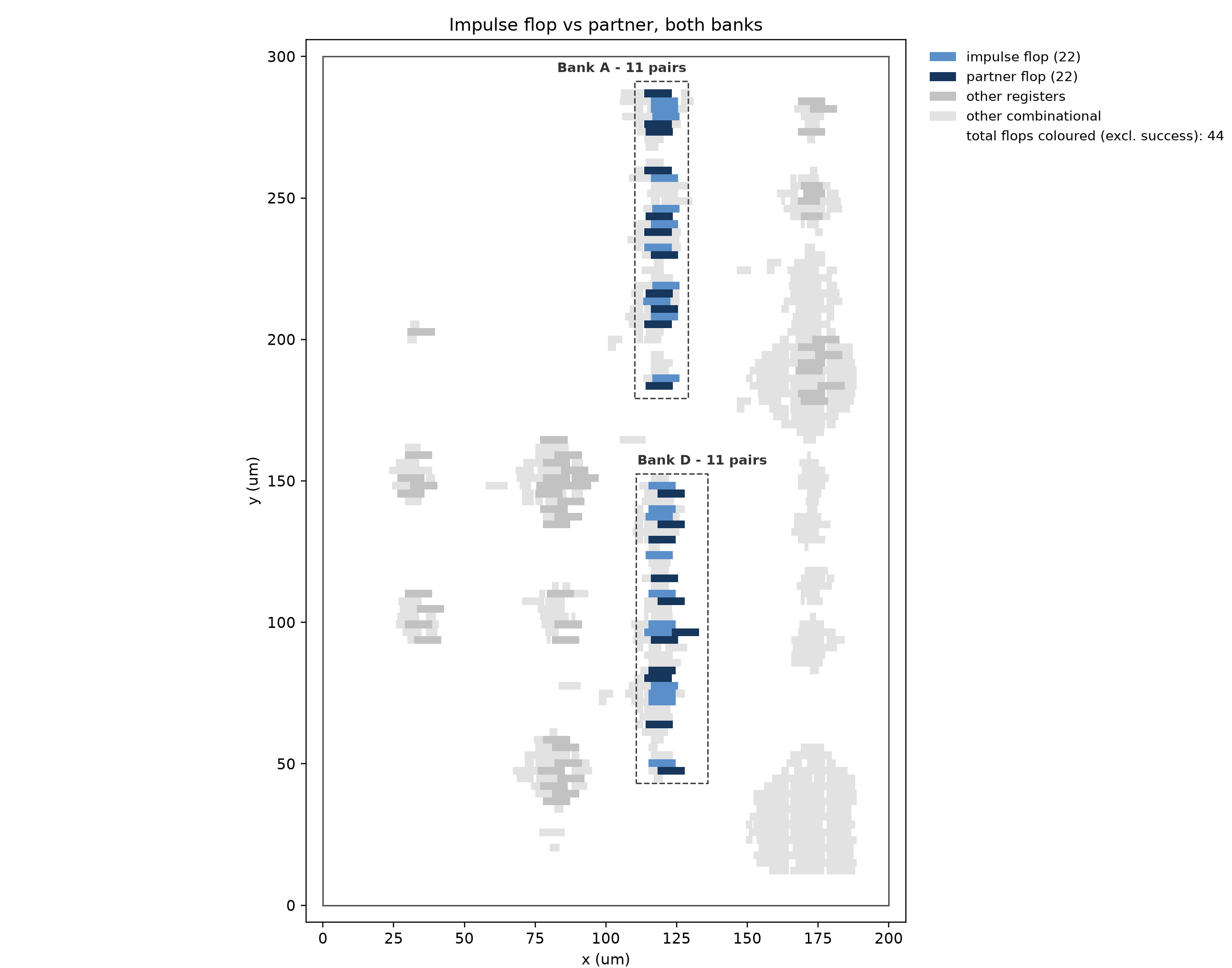
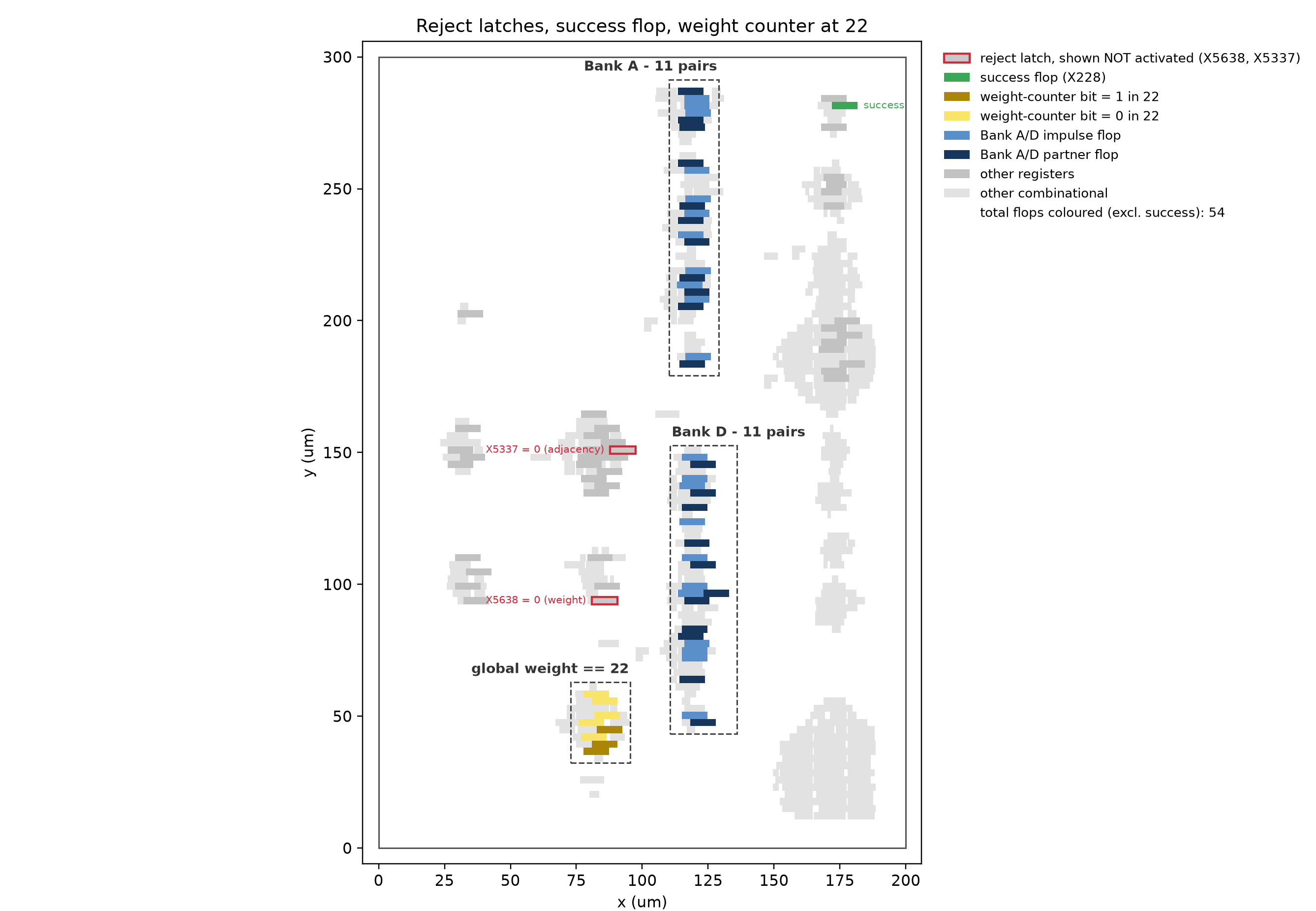
This match corresponded with each counter pair set at a count of 2. I then added the two format latches in their passing state (off), and setting each group to a count of 2 subsequently set the global counter with the value 22 which I also included in the image as flops in that region were also part of the required state. That accounted for 54 of the flops, all agreeing with the required state.
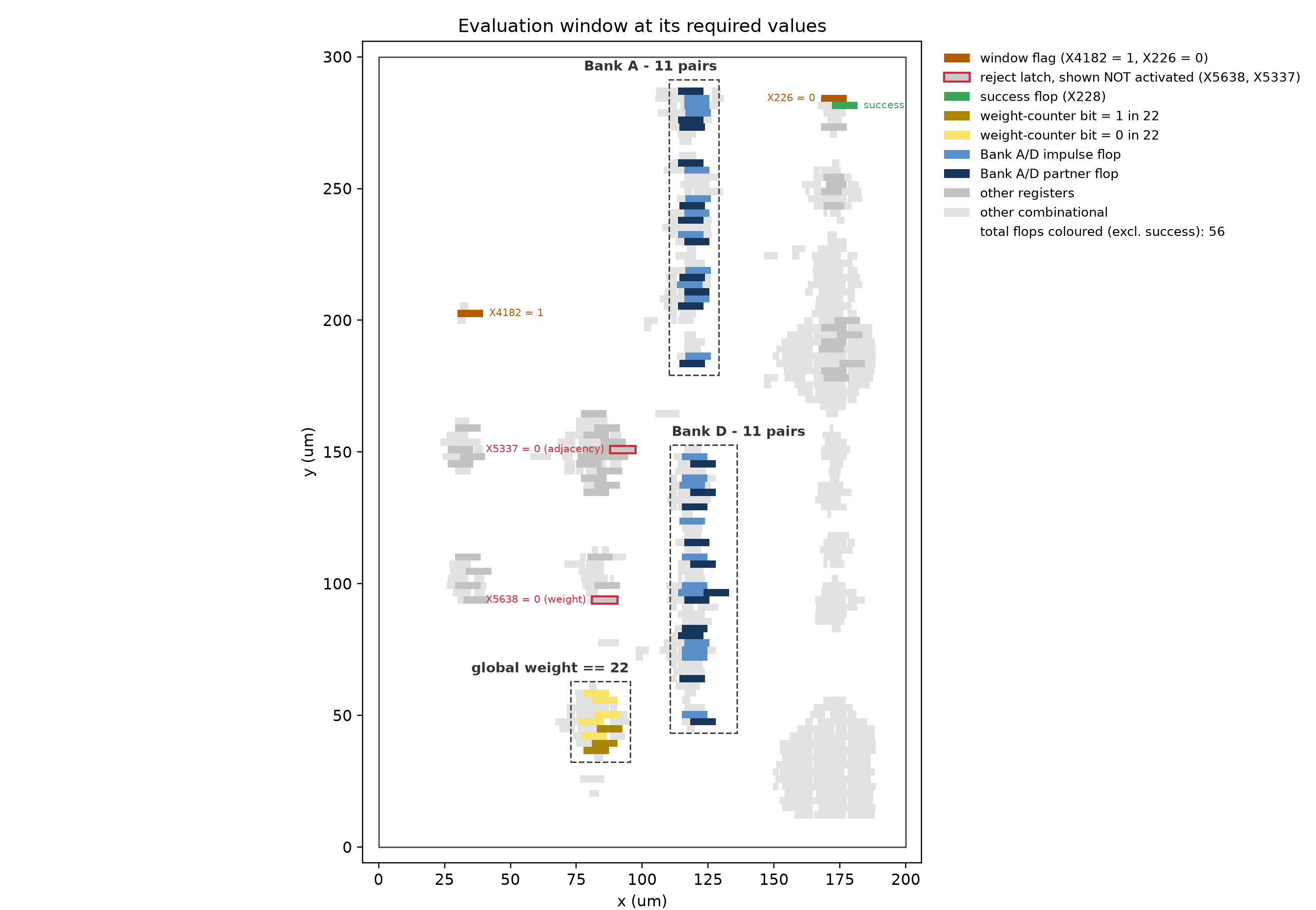
Finally, I added the two evaluation window flags at their required values. That brought it to 56, the full size of the required state.
Diffing my constructed state against required_state.json gave 56 of 56 in
agreement, 0 disagreements. What I had built with reasoning was the required state.
This was really a check from two directions. The required state came backwards, pushing success = 1 through 47 gates. The impulse map plus the counters built the same 56 bits forwards. Two unrelated derivations agreeing 56 of 56 with 0 disagreements is confirmation, not a coincidence.
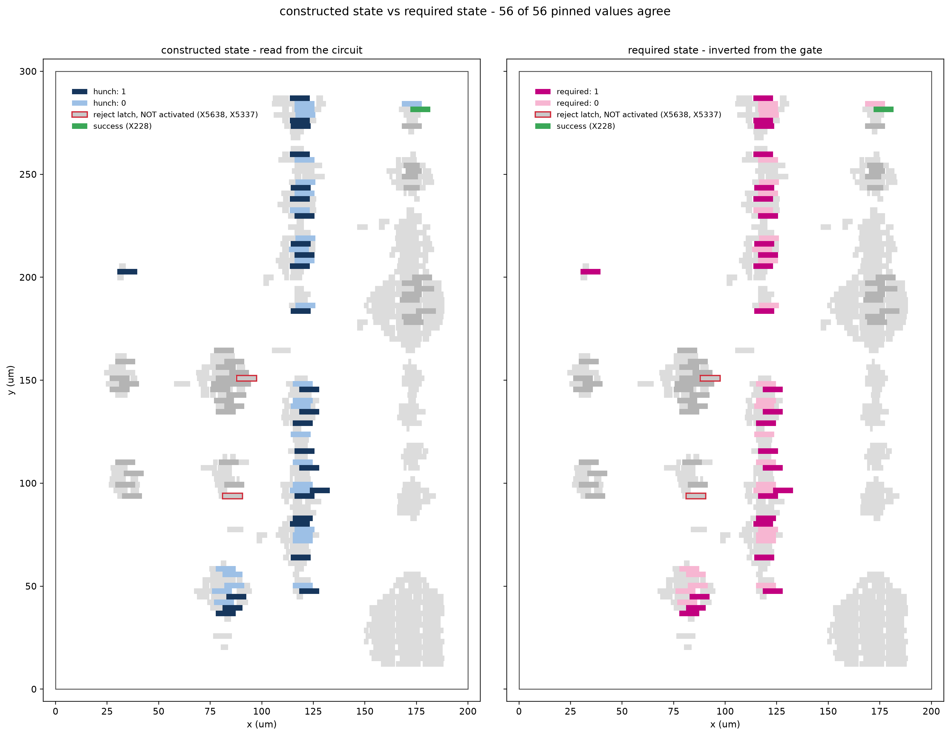
Thefore, gathering all of my thoughts and findings together, the required state can we worded into a condition on the input. The condition says that: every group must have been hit exactly twice, both latches off, the global count at 22 and the window open. This collapsed the problem to a few rules on the grid:
- Exactly 2 per row. The weight latch
X5638. - Exactly 2 per column. Bank A is the columns, each must read 2.
- Exactly 2 per Bank D region. Each of the eleven regions must read 2.
- No two 1s touching, in any of the 8 directions. The adjacency chain.
Hence I ran a depth first search over the rows, placing two 1s per row and discarding any branch that broke a column, region or adjacency rule. It returned exactly one grid:
col:  0  1  2  3  4  5  6  7  8  9 10

Grid:
      0  0  0  0  0  0  0  1  0  1  0
      1  0  0  0  0  1  0  0  0  0  0
      0  0  0  0  0  0  0  1  0  1  0
      1  0  1  0  0  0  0  0  0  0  0
      0  0  0  0  1  0  1  0  0  0  0
      0  0  1  0  0  0  0  0  1  0  0
      0  0  0  0  1  0  0  0  0  0  1
      0  1  0  0  0  0  1  0  0  0  0
      0  0  0  1  0  0  0  0  0  0  1
      0  0  0  0  0  1  0  0  1  0  0
      0  1  0  1  0  0  0  0  0  0  0
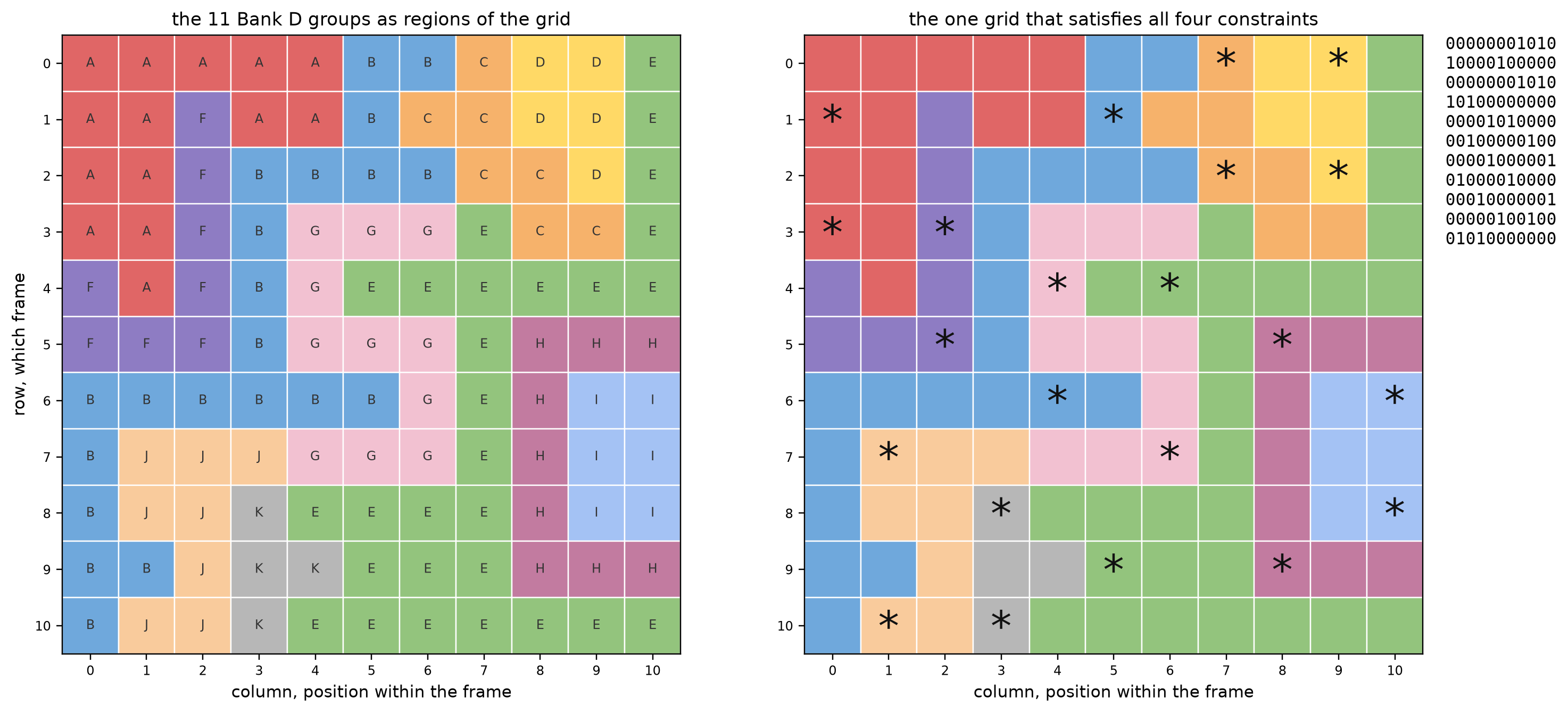
Feeding that grid into the viewer, on the netlist pulled straight from the GDS, we get this output:
decoded message : '(* TWO STARS *)'
success asserted: True
The overall lesson: visual aids really do help a lot :). But really though, these visualisations and the interactive suite AI helped me to build allowed me to iterate through various ideas quickly, whilst also deepening my understanding of the chip everytime I ran something.
What the puzzle actually is
In hindsight, after I had solved the puzzle and done some research, this circuit is simply a checker for a game. It is Two Not Touch, aka Star Battle. You take a grid split into regions and place two stars in every row, every column and every region, with no two stars touching in any of the eight directions. Looking back, those are the exact four constraints I had recovered the hard way.
The Bank D flops simply represented the regions of the grid. Each pair counted how many stars sat in its region, so every region had to read two. The chip even says it in the output: (* TWO STARS *). Additionally, all the easter eggs point towards this same thematic similarity with the stars.
Easter eggs
There are probably more easter eggs (and I will update the page if I find any more). These are the ones I found:
Morse code at the bottom of the die
While viewing the chip in various online GDS viewers, I noticed a thin line below the die. It sits on layer 200/0, at y = -52.72, just under the design boundary. The row runs almost the full width of the chip. Some viewers do not draw it, since layer 200/0 is not a sky130 layer and it sits off screen below the die. Nonetheless, here is a screenshot of the morse code using this GDS viewer. Just remember to slightly zoom out and look below the chip.

Zooming in, the line is a row of dots and dashes. It is morse code.
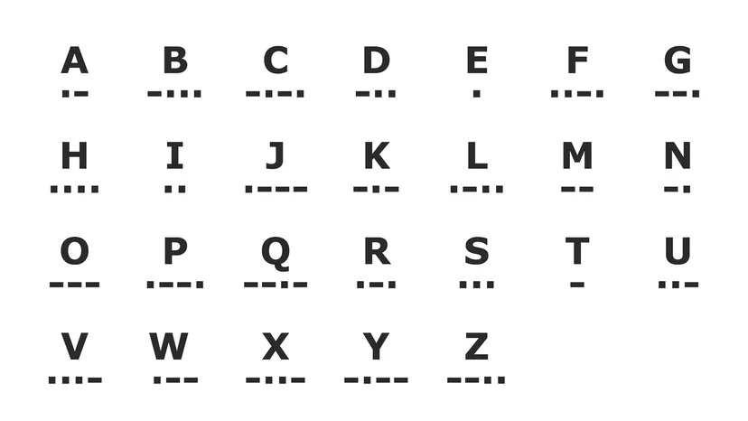
Decoding it left to right gives “PER ARENAM AD ASTRA”. Seems like some sort of Latin phrase. A quick search reveals that it is a play on “per aspera ad astra”, through hardships to the stars, with arenam meaning sand in place of silicon. It translates as through sand to the stars. The pun fits the theme of an actual chip, since silicon is refined from sand and we place stars in a grid.
The night sky awaits
The original repo also provides an example_inputs.vcd, the sample input waveforms. While investigating the example inputs to the chip, I wrote a small Python parser to pull the serial input I out of it, sampling one bit on each positive clock edge while enable was high. Since each attempt was 121 bits, I split each attempt into 11 frames of 11 bits. I then discovered, in each frame, the first 7 bits are one ASCII character, read LSB first. The last 4 bits are just zero padding. Reading them out gave 11 ASCII characters per attempt. The two example attempts came out as “The night s” and “ky awaits “, so together they spell “The night sky awaits”. It thereby carries the same night sky theme as the morse line and first prompted me into testing various ascii inputs with zero padding as a solution to this puzzle.
Other messages the machine streams
Along the way I fed the chip some extreme inputs just to see what it would say. An empty grid of all zeros streams “EMPTY SKY”:
  cycle  0: 01000101  0x45  'E'
  cycle  1: 01001101  0x4D  'M'
  cycle  2: 01010000  0x50  'P'
  cycle  3: 01010100  0x54  'T'
  cycle  4: 01011001  0x59  'Y'
  cycle  5: 00100000  0x20  ' '
  cycle  6: 01010011  0x53  'S'
  cycle  7: 01001011  0x4B  'K'
  cycle  8: 01011001  0x59  'Y'
  decoded message : 'EMPTY SKY'
  success asserted: False
And a full grid of all ones streams “BIG BANG”:
  cycle  0: 01000010  0x42  'B'
  cycle  1: 01001001  0x49  'I'
  cycle  2: 01000111  0x47  'G'
  cycle  3: 00100000  0x20  ' '
  cycle  4: 01000010  0x42  'B'
  cycle  5: 01000001  0x41  'A'
  cycle  6: 01001110  0x4E  'N'
  cycle  7: 01000111  0x47  'G'
  decoded message : 'BIG BANG'
  success asserted: False
However, both are reject messages since success is never asserted.